 首页 - 电子元器件 - ST(意法半导体) - GPS用IC - GPS解决方案

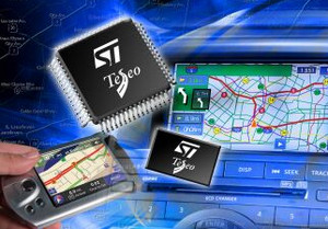
Teseo
Teseo 平台是一个高灵敏度的,独立的GPS解决方案,它是消费者,手持设备,PND(便携式导航设备),车载导航和远程信息处理系统的理想选择。嵌入式快闪记忆体,满足了设备制造商定制其所需要的接口之后,再负载整个 GPS 软件(包括跟踪,采集,导航和数据输出)的需求。
Teseo II
eseo II 是业界第一款单芯片的能够接受来自多个卫星导航系统信号的定位设备,这些卫星导航系统包括:GPS、伽利略、GLONASS 和 QZSS 导航系统。Teseo II 家族结合了定位高精度,和具有强大处理能力与出色的设计灵活性的室内感光性能。
ST最新的定位 SoC 适合广泛的消费人群和汽车应用,包括个人导航设备,导航系统模块,船用设备,健身器材,汽车导航,远程信息处理,紧急呼叫和先进的驾驶辅助系统。
Cartesio?
Cartesio 是一个嵌入了 GPS 的应用处理器。这个片上系统通过把 ARM9 主机处理器容量,高性能的 32 通道 GPS 相关器和大量的外设和接口集结合在一起,降低了最终的应用成本。 ST 的 Cartesio 为 PND、车载导航、车载智能通信系统、高级音频和连接应用提供解决方案。
Cartesio+
Cartesio+ 是 Cartesio 家庭的新型应用处理器,为下一代车载和便携式导航系统嵌入了GPS系统。结合了 ARM1176 的超级处理能力、定位精度和丰富的集成外部设备,ST 的 Cartesio+ 可实现成本与空间高效的导航与用户高体验性的信息娱乐应用。 Cartesio+ 是一种具有两不同功能组合的扩展器件。 STA2064 和 STA2065 分别适用于物料单 (BOM) 敏感与高性能要求的应用。
STA2058
Description
STA2058 is the high-sensitivity baseband of TESEO GPS platform which include the STA5620 RF Front-End.
The embedded Flash memory enables the equipment manufacturer to load the entire GPS software (including tracking, acquisition, navigation and data output) after customizing its interfaces to his needs. A standard GPS library is available from ST.
TESEO is the ideal solution for consumer, handheld, PND (portable navigation), in vehicle navigation and telematics systems.
SBAS (WAAS and EGNOS) feature is also supported.
Key Features
Single chip baseband with embedded Flash
Complete embedded memory system:
Flash 256 KB +16 Kbytes
RAM 64 Kbytes
66 MHz ARM7TDMI 32 bit processor
High performance GPS engine (HPGPS)
SBAS (WAAS and EGNOS) supported
Sensitivity (-146 dBm acquisition, -159 dBm tracking)
Time to first fix (1s reacquisition, 2.5 s hot start, 34 s warm start, 39 s cold start)
Accuracy (2 m autonomous)
External memory interface (EMI) supporting up to 64 Mbite of external SRAM, Flash and ROM
Extensive GPS receiver interfaces: 48 GPIOs, 4 UARTs, 2 SPIs, 2 I2Cs, 2 CANs 2.0, 1 USB 1.1,1 HDLC and 4 channels ADC
ST proprietary Flash embedded technology
LFBGA144 and LQFP64 lead-free package
-40 °C to 85 °C operating temperature range
Evaluation kits
STA2058 module reference design (25x25mm)
Evaluation board hosting STA2058 module
SDK board (for application SW development)
STA2062
Description
The STA2062 is an highly integrated SOC application processor combining host capability with embedded GPS.
STA2062 targets in vehicle and mobile navigation (PND), telematics, advance audio and connectivity systems.
Key Features
High performance ARM926 MCU (up to 333MHz)
MCU memory organization
Cache: 16KByte instruction, 16KByte data
8KByte instruction TCM (tightly coupled memory)
8KByte data TCM
32KByte embedded ROM for boot
Two banks of 64KByte embedded SRAM
512Byte embedded SRAM for back-up
4GByte total linear address space
Memory extension through:
Flexible static memory controller-FSMC (NOR/NAND Flash, CF/CF+, ROM, SRAM support)
Mobile DDR/SDRAM controller: 16bit data @166MHz, 2 Chip Select, 512Kbit each
Interrupt
64-channel interrupt controller (VIC)
16-vectorized interrupts with 16 programmable priority Level
DMA
Two 8-channel double port system DMA controllers
32 DMA request for each controller
Two external DMA requests are supported
32 channel high performance GPS correlation embedded subsystem
Eight 32-bit free running timers/counters
Four 16-bit extended function timer (EFT) with input capture/output compare and PWM
Real time clock (RTC)
Pulse width light modulator (PWL)
32-bit watchdog timer
Four autobaud UART with 64X8 transmit and 64x12 receive FIFO with DMA and hardware flow control
One IrDA(SIR/MIR/FIR) interface
Three I2C multi-master/slave interfaces
Two synchronous serial port (SSP) with 32x32 separate transmit and receive FIFO with Motorola-SPI, National-MicroWire and Texas-SSI support modes
Four multichannel serial ports (MSP) with 32x8 separate transmit and receive FIFO
Color LCD controller for STN,TFT or HR-TFT panels
USB 2.0 OTG high speed dual role controller (ULPI interface)
USB full speed dual role controller with integrated 1.1 physical layer transceiver
Two secure-digital multimedia memory card Interface (SD/SDIO/MMC) up to 8 bit data
SPDIF input interface
C3 hardware Reed-Solomon decoder
Hardware sample rate converter (SaRaC)
Four 32-bit GPIO ports
JTAG based in-circuit emulator (ICE) with embedded medium trace module
Typical working condition: Vdd: 1.2 ±10%V, VIO: 1.8V
Overdrive: Vdd: 1.4 ±5%V, VIO: 1.8 ±10%V, 2.5 ±10%V
Bus frequency: 166 MHz (overdrive)
Bus/DDR frequency: 166 MHz
HCMOS 0.90μm process
Package:
LFBGA16x16x1.4mm (19x19balls)
0.8mm ball pitch, (0.4mm ball)
Full array
Ambient temperature range: -40 / +85°C
STA2062A
Key Features
High performance ARM926 MCU (up to 333 MHz)
MCU memory organization
Cache: 16 Kbyte instruction, 16 Kbyte data
8 Kbyte instruction TCM (tightly coupled memory)
8 Kbyte data TCM
32 Kbyte embedded ROM for boot
Two banks of 64 Kbyte embedded SRAM
512 Byte embedded SRAM for back-up
4 Gbyte total linear address space
Memory extension through: Flexible static memory controller-FSMC (NOR/NAND Flash, CF/CF+, ROM, SRAM support) Mobile DDR/SDRAM controller: 16 bit data @166 MHz, 2 Chip Select, 512 Kbit each
Interrupt
64-channel interrupt controller (VIC)
16-vectorized interrupts with 16 programmable priority level
DMA
Two 8-channel double port system DMA controllers
32 DMA request for each controller
Two external DMA requests are supported
32-channel high performance GPS correlation embedded subsystem
Eight 32-bit free running timers/counters
Four 16-bit extended function timer (EFT) with input capture/output compare and PWM
Real-time clock (RTC)
Pulse width light modulator (PWL)
32-bit watchdog timer
Four autobaud UART with 64X8 transmit and 64x12 receive FIFO with DMA and hardware flow control
One IrDA(SIR/MIR/FIR) interface
Three I2C multi-master/slave interfaces
Two synchronous serial port (SSP) with 32x32 separate transmit and receive FIFO with Motorola-SPI, National-MICROWIRE and Texas- SSI support modes
Four multichannel serial ports (MSP) with 32x8 separate transmit and receive FIFO
Color LCD controller for STN,TFT or HR-TFT panels
USB 2.0 OTG high speed dual role controller (ULPI interface)
USB full speed dual role controller with integrated 1.1 physical layer transceiver
Two secure-digital multimedia memory card interface (SD/SDIO/MMC) up to 8 bit data
SPDIF input interface
C3 hardware Reed-Solomon decoder
Hardware sample rate converter (SaRaC)
Two controller area network (CAN)
Four 32-bit GPIO ports
JTAG based in-circuit emulator (ICE) with embedded medium trace module
Typical working condition: Vdd: 1.2 V ±10%, VIO: 1.8 V
Overdrive: Vdd: 1.4 V ±5%, VIO: 1.8 V ±10%, 2.5 V ±10%
Bus frequency: 166 MHz (overdrive)
Bus/DDR frequency: 166 MHz
HCMOS 0.90 μm process
Package:
LFBGA16x16x1.4 mm (19x19 balls)
0.8 mm ball pitch, (0.4 mm ball)
Full array
Ambient temperature range: -40 / +85 °C
