 首页 - 电子元器件 - ST(意法半导体) - GPS用IC - RF前端接收器

STA5620 是一种全集成 RF 前端,可将 GPS L1 信号由 1575.42 MHz 下变频为 4.092 MHz。 接收器出色的噪声系数和线性保证恶劣环境下具有优异的接收质量。 片上振荡器晶振频率 10 MHz 至 40 MHz。 本器件支持温补振荡器(TCXO),并具有振荡器频率缓冲拷贝功能。
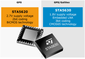
主要特点 ?低 IF 架构 (单一下变频 4f0)?与 L1 GPS 和 Galileo 信号兼容?2.7 V 电压 ?采用 ST BiCMOS6G 专有技术 (45 GHz 双极型,0.35 μm CMOS) ?2 kV HBM ESD 保护 STA5630 是一种全集成 RF 前端,可将 GPS L1 信号由 1575.42 MHz 下变频为 4.092 MHz。 这款芯片嵌入高性能 LNA,减少外部元器件数量。 芯片采用先进 的 CMOS 65 nm 工艺。 3位模数转换器 (ADC) 可将 IF 信号转换为符号 (SIGN) 与幅度信号 (MAG0 和 MAG1)。 内部集成振幅位,用以控制可变增益放大器。 VGA 增益还可以通过 SPI 接口设置。
STA5620A
Description
The chip is a fully integrated RF front-end able to down-convert the GPS L1 signal from 1575.42 MHz to 4.092 MHz.
The IF signal is converted by a two bit ADC. Sign (SIGN), Magnitude (MAG) and the 16.368 MHz sampling clock (GPS_CLK) are provided to the baseband.
The magnitude data is internally integrated in order to control the variable gain amplifiers in accordance to the RF input signal strength.
An excellent quality of reception in critical environments is ensured by the good noise figure and linearity of the receiver.
The on-chip oscillator supports crystal frequencies in the range of 10 MHz to 40 MHz. It is able to support TCXO providing also a buffered copy of the oscillator frequency.
The chip, using STMicroelectronics BiCMOS SiGe technology, is housed in a QFN-32 package.
Key Features
Low IF architecture (fIF= 4fO)
Minimum external components
VGA gain internally regulated
On chip programmable PLL
Typ. 2.7 V supply voltage
SPI interface
2 kV HBM ESD protected
Compatible with GPS L1
Standard QFN-32 package
Low power for portable designs
STA5620C
Description
The chip is a fully integrated RF front-end able to down-convert the GPS L1 signal from 1575.42 MHz to 4.092 MHz.
The IF signal is converted by a two bit ADC. Sign (SIGN), Magnitude (MAG) and the 16.368 MHz sampling clock (GPS_CLK) are provided to the baseband.
The magnitude data is internally integrated in order to control the variable gain amplifiers in accordance to the RF input signal strength.
An excellent quality of reception in critical environments is ensured by the good noise figure and linearity of the receiver.
The on-chip oscillator supports crystal frequencies in the range of 10 MHz to 40 MHz. It is able to support TCXO providing also a buffered copy of the oscillator frequency.
The chip, using STMicroelectronics BiCMOS SiGe technology, is housed in a QFN-32 package.
Key Features
Low IF architecture (fIF= 4fO)
Minimum external components
VGA gain internally regulated
On chip programmable PLL
Typ. 2.7 V supply voltage
SPI interface
2 kV HBM ESD protected
Compatible with GPS L1
Standard QFN-32 package
Low power for portable designs
STA5630
Description
The chip is a fully integrated RF front-end able to down-convert either the GPS L1 signal from 1575.42 MHz to 4.092 MHz.
The STA5630 embeds high performance LNA minimizing external component count. The chip uses state of the art CMOS 65 nm technology.
A 3-bit ADC converts the IF signal to Sign (SIGN) and Magnitude (MAG0 and MAG1). The magnitude bits are internally integrated in order to control the variable gain amplifiers. The VGA gain can be also set by the SPI interface.
The STA5630 accepts a range of reference clocks (10 to 52 MHz) and generates a 16.368 MHz sampling clock (GPS_CLK) for the baseband. The STA5630 embeds LDO to supply the internal core of the device facilitating requirements to external power supply.
High performance low power and cost effective device, the STA5630 is the ideal solution for automotive, cellular and consumer battery powered applications.
Key Features
Integrated LNA
Low power consumption (<25 mW)
1.8 V supply voltage
GPS and Galileo compliant
Minimum external components
Serial interface
3 bits A/D converter
CMOS 65 nm technology
Standard QFN-32 package
